Breakdown Voltage: Breakdown Voltage (VBR) is the maximum reverse bias that can be applied, beyond which the diode readily conducts current. Exceeding the breakdown voltage with no current-limiting protection can cause severe device degradation.
Dark Current: Usually abbreviated as ID. The current flowing through a reverse biased photodiode when light is not incident upon a photodiode. Higher reverse bias voltages result in higher dark currents. Dark Current can be minimised by proper device design and is not present in zero photodiode bias circuits (see shunt resistance).
Detectivity: Detectivity (D*) is a measure of detector signal-to-noise ratio (SNR), normalised for detector active area:
D* = A½/NEP where A is the active area, and NEP is the Noise Equivalent Power.
Detectivity values from 1012 to 1014 cmHz½/W can be expected for silicon photodiodes.
Frequency Response: The frequency response of a photodiode is deemed as the point where the photocurrent has decreased by 3dB (0.7) of the low frequency response. Maximum frequency response can be calculated from the formula:
fmax = 0.35/tr where tr, is rise time.
Full-Width-Half-Max: Usually abbreviated as FWHM. Used most commonly when discussing beam angle or spectral bandwidth. In both cases it refers to the distance from 50% to 50% point, or –3dB to –3dB point. Beam angle value is specified in degrees and spectral bandwidth values are specified in nanometres.
Junction Capacitance: The p-n junction has a capacitance (CJ) similar to a parallel-plate capacitor - two highly conductive semiconductor regions separated by a resistive depletion layer. The Junction Capacitance is directly proportional to the active area. In the case of photodiodes, the Junction Capacitance can be reduced by reverse biasing. The Junction Capacitance in conjunction with the inherent series resistance of the diode is not the limiting factor for response time of the device (see response time). It can be minimised by device design.
Noise Current: Photodiode Noise Current (I*N) consists of two main components: Shot Noise and thermal (Johnson) noise. The Shot Noise is calculated from the formula:
I*S = (2qIDRB)½
where I*S is the Shot Noise current in Amperes (rms), q is the electron charge (1.6x10⁻¹⁹ coulombs), ID is the Dark Current in Amperes, and B is the operating bandwidth in Hz. With no reverse bias, the Dark Current and the Shot Noise are both zero.
The standard thermal noise equation shows that a high shunt resistance (RSH) provides low noise:
IT = (4kTB/RSH)½
where IT is the thermal noise current in Amperes (rms), k is Boltzmann's constant (1.38x10⁻²³ Joules/°K), T is the temperature in °K, RSH is the shunt resistance in ohms, and B is the operating bandwidth in Hz.
The total noise current is the quadrature sum of the thermal and shot noise. Typical noise current values range from 10-12Arms/(Hz)½ for large area devices designed for high output current, to 10-15Arms/(Hz)½ for smaller devices optimised for low noise.
Noise Equivalent Power: Noise Equivalent Power (NEP) is the incident light power for which the signal-to-noise ratio (SNR) is equal to one, and thus is the measure of the minimum detectable light power.
NEP = I*N/R
where R is the responsivity and I*N is the noise current. Photodiode NEP values range from about 10-15 Watts rms/(Hz)½ for small area, low noise silicon photodiodes to over 10-12 Watts rms/(Hz)½ for very large cells. Normally it is assumed that the NEP depends solely on the Shot Noise and thermal Johnson noise.
Open-Circuit Voltage: Open-Circuit Voltage (VOC) is the voltage generated by a photodiode across a very large load resistor when the diode is illuminated. VOC is usually of interest when it is desirable to have the voltage drop (VL) across the resistor proportional to the light level. VL is linear with the light level as long as VL is much less than VOC. The use of a load resistor is not recommended because it is slower, noisier, and less linear than short circuit current operation.
Operational Amplifier/Photodiode Combination Linearity: The operational amplifier, when used as a current-to-voltage converter, provides a unique solution to the linearity limitations imposed on photodiodes by the terminating load impedance. In this transimpedance configuration, the photodiode views a load impedance as Za, as shown in the following equation:
Za = Rf/(A[1+(ωRfCf)2]½)
where A is the photosensitive active area, ω is the operating frequency, Rf is the feedback resistance and Cf is the feedback capacitance.
This equation shows that, at low frequencies, the apparent photodiode load impedance is very low, but increases with increasing frequency. With the availability of open-loop amplifier gains that exceed 105 at DC, it is evident that photodiode signal gain can be accomplished over a reasonable frequency range without the loss of response linearity. A good approximation of the photodiode/operational amplifier response linearity can be determined by the substitution of Za for RL in the linearity equations for both photovoltaic and photoconductive modes.
It is important to remember that operational amplifiers do not have the same dynamic range as a silicon photodiode, and that the linearity range may be limited by the amplifier. If an amplifier has an rms noise voltage of 1mV at the output, and a maximum output of 13V (+ 15V supply), then this is a maximum range of just over four decades. If the output signal voltage is limited to 100mV (100:1 S/N) at the low end, and 10V at the high end, this is only two decades of linear output signal voltage. This linear range limitation makes the proper choice of feedback resistor value an important design consideration.
Operational Amplifier Transimpedance: When used in conjunction with a silicon photodiode, an operational amplifier is used in the transimpedance mode as a current-to-voltage converter. In this mode, the photo current, or dark current, is converted to a voltage by an impedance in the feedback loop. When operating at DC, the output signal voltage is proportional to the feedback resistor value and can be calculated from the formula:
Eout = IinRf
where Iin is the photodiode current and Rf is the feedback resistance. This formula does not consider any offset voltages.
Optical Absorption: Optical absorption, and its associated absorption depth, are properties of the semiconductor material from which the photodiode is manufactured. Their value indicates the thickness of silicon required to absorb, and therefore detect, the incident light of a given wavelength.
Photoconductive Detector: When a photodiode is used with a reverse bias, it is said to be used in the photoconductive mode. This terminology probably originated when the photodiode was first used in place of true photoconductive detectors, such as cadmium sulphide detectors. This term is actually a misnomer, since the photodiode is a current source, with or without bias. Using a reverse bias improves the detector's linearity, speed of response and capacitance. It increases the noise level of the diode itself compared to zero bias, but can lower the system noise level due to lower input capacitance to the electronics.
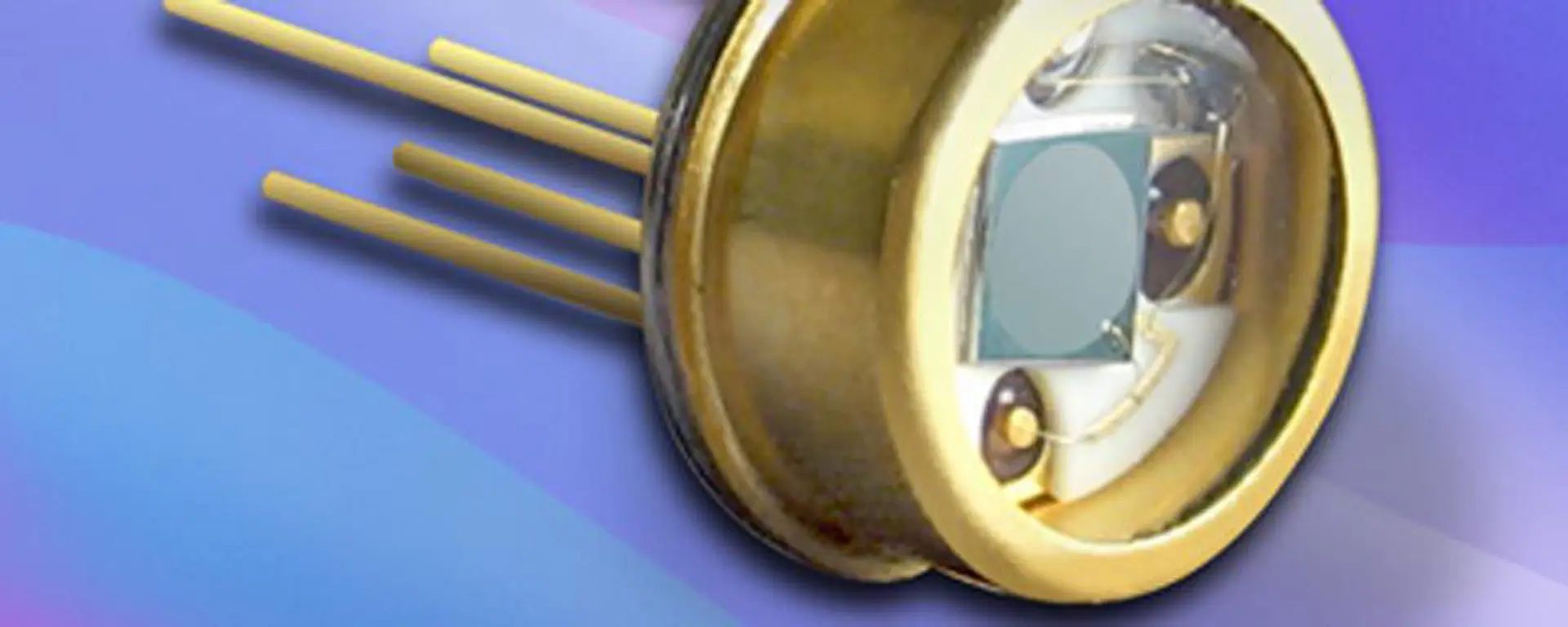
Photodiode: Generic name given to any diode used as a light detector. Device has no internal gain like a photodiode or photodarlington. Directly converts photons (light) into electrons (current). It is linear over at least 6 decades of light input. Average saturation point is 10mW/cm2. Used extensively where light must be accurately measured or higher speed (greater than 30kHz) is required. Measured in Amps/Watt (A/W).
Photometric Response: Photometric response, measured in amperes per lumen, is the responsivity of the photodiode, modified to the eye's spectral response. Since most common light sources emit more power outside the visible spectrum than inside it, and since silicon photodiodes are more sensitive at longer wavelengths than in visible light, this parameter is not appropriate for most applications. See short-circuit current and responsivity.
Photovoltaic Detector: When a photodiode is used without a reverse bias, it is said to be used in the photovoltaic mode. This terminology probably originated when the photodiode was first used in place of true photovoltaic detectors, such as thin silver layers deposited on non-crystalline silicon. This term is actually a misnomer, since a silicon photodiode is a current source, with our without a reverse bias. Photovoltaic mode is the most common method of use, because there is no dark current to offset the signal current, and the noise levels and speed of response are usually more than adequate. Note that small input voltage offsets of the electronics to which the detector is connected will produce small offset currents.
Quantum Efficiency: External quantum efficiency (EQE) is the percentage of incident power which results in an electric current which flows when an external load is connected to the photodiode. Quantum efficiency can be calculated with the formula:
EQE = 1.24R/λ
where EQE is the percentage of external quantum efficiency, R is the photodiode responsivity measured in amperes/watt, and λ is the wavelength in microns.
Typical values of quantum efficiency range from 50% to 95%, depending on the wavelength of the incident light and the type of photodiode. EQE is less than unity because of reflection losses at all wavelengths, surface loss mechanisms at near-UV wavelengths, and poor absorption of photons at near-IR wavelengths.
Radiant Intensity: Radiant measurement of on axis intensity. This value must be known to calculate optical power incident on a detector that is greater than 15cm from the LED. The angle of measurement is a critical component when comparing data sheets from one vendor to the next.
Response Linearity: Silicon photodiode response is usually linear to within a few tenths of a percent from the minimum detectable incident power up to several milliWatts per square centimetre. Response linearity improves with increasing applied reverse bias and decreasing effective load resistance.
Response Uniformity: The uniformity of response is dependent upon the qualities of the window cap and the photo diode front and rear surfaces. In applications where the operating wavelength is less than approximately 800 nm, the quality of the diode front surface is most important. The response uniformity is inversely proportional to the illuminated area, therefore, surface condition is critical in situations where a small light spot is used. The rear surface is reflective, and its consistency is a key factor in long wavelength applications.
At wavelengths longer than approximately 800nm, the rear surface quality dominates the photodiode. Photons start to penetrate the silicon deep enough to reach the back surface.
Responsivity (Radiometric Responsivity): Photodiode responsivity (R) is the ratio of the photocurrent generated for every Watt of incident light power in units of ampere/Watt (A/W or mA/mW). Responsivity is the preferred measure of a photodiode's response to light. See also quantum efficiency.
Response Time: Response Time (τR), also known as the rise and fall time, is a measure of the period of time it takes an emitter or detector to go from the 10%-90% point, emitting and detecting respectively, or the 90%-10% point. In photodiodes Response Time is affected by the wavelength (the shorter the wavelength, the faster the response), capacitance, load resistance and transition time of the silicon. RC time constant of the device is almost never the limiting factor. The speed of the device is almost always due to the transit time of the semiconductor material and the distance from the depletion region to edge of device. The response time can be shortened by increasing the bias voltage, thus decreasing the junction capacitance of the device, lowering the RC time constant, and decreasing the transition time through the silicon.
Series Resistance: Series resistance (RS) of a photodiode is the resistance of the detector through which the photodiode current must flow. It depends upon material properties and device design, as well as the quality of the electrical contacts to the device. RS is low enough to be of no concern for the majority of photodiode applications.
Short-Circuit Current: Short-circuit current (ISC) is the current generated by a photodiode into a short circuit when the diode is illuminated. ISC depends strongly on the intensity and spectral distribution of the light source. See responsivity.
Shunt Resistance: Shunt resistance (RSH) is the zero-bias resistance of a dark photodiode. The equivalent resistance is an important performance parameter for photodiodes, since it puts a lower limit on the noise level of the device. It is determined by placing a small reverse bias test voltage (typically 10mV) on the photodiode and measuring the current. The ratio of the values of the measured current and the test voltage is the shunt resistance (see also Noise Equivalent Power). This value must be known to determine noise current generated by the photodiode in a photovoltaic, short circuit current mode circuit. Shunt resistance is sometimes called source impedance.
Spectral Response: The conventional method for determining the sensitivity of photodiodes. Expressed in Amps/Watt (A/W). The monochromatic wavelength the measurement is done at must also be specified. Silicon photodiodes are sensitive to light in the spectral range from less than 200nm in the ultraviolet (UV), through the visible, to about 1100nm in the near infra-red (NIR). Special device designs can optimise the responsivity at any wavelength, especially in the UV and NIR. Window materials degrade the spectral response range of the detector assembly compared to bare chips because of reflection and absorption.


