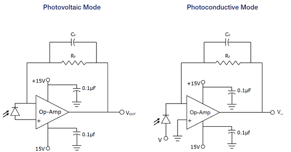


For most applications, a transimpedance (current-to-voltage) amplifier is recommended to allow the photodiode to operate in a virtually short circuit condition, thus retaining its linear response. Generally speaking, a photovoltaic (zero bias) circuit is used in applications where speed is not important. Biasing the photodiode (photoconductive operation) increases the speed, reduces junction capacitance and improves the linearity of the photodiode.
The feedback resistor must be chosen carefully because it will affect the output range and bandwidth of the circuit. Before choosing a resistor, the minimum/maximum light input signal, the number of decades of dynamic range desired, and the bandwidth all need to be considered. Following are formulas useful for designing a transimpedance amplifier circuit.
Output Voltage (Vout)
|
Vout |
= ISRF |
||
|
= RPORF |
where IS = |
Photodiode light signal current |
|
|
RF = |
Feedback Resistance | ||
| R = | Responsivity at wavelength of irradiance, A/W | ||
| PO = | Light power incident on photodiode active area, W |
Feedback Capacitor (CF)
| CF | = 0.5πfRF | where f = | Maximum operating frequency, Hz |
| RF = | Feedback resistance |
Gain Bandwidth Product (GBP)
In order to maintain circuit stability at the frequency and gain chosen, an operational amplifier with a sufficiently high Gain Bandwidth Product must be chosen. This can be calculated using the formula:
| GBP | = 2f²πRF(CF+CJ) | where f = | Maximum operating frequency, Hz |
| RF = | Feedback resistance | ||
| CF = | Feedback capacitance | ||
| CJ = | Junction capacitance of the photodiode |